Modern games emphasize graphics, and their install size can now exceed 100 GB. To access this huge amount of data, the processing speed depends on the specifications of the graphics card (GPU) and, in a certain extent, other components of your system.
On the GeForce RTX 40 series graphics cards, NVIDIA has introduced new innovations to speed up the process, ensuring smooth games and faster frame rates, thus avoiding texture loading issues or other interruptions.
The important role of caching
GPUs are equipped with high-speed memory caches, located near the GPU processing cores. These caches store data that is likely to be needed. When the GPU can fetch data from these caches rather than requesting it from VRAM (video memory, located farther away) or system RAM (even farther away), then data is accessed and processed faster. This results in improved performance, increased game fluidity and reduced power consumption.
GeForce graphics cards are equipped with Level 1 (L1) cache in each Streaming Multiprocessor (SM). Each GeForce RTX 40 Series Graphics Processing Cluster (GPC) can contain up to twelve of these SMs. Then there is a larger, shared level 2 (L2) cache, which can be quickly accessed with minimal latency.
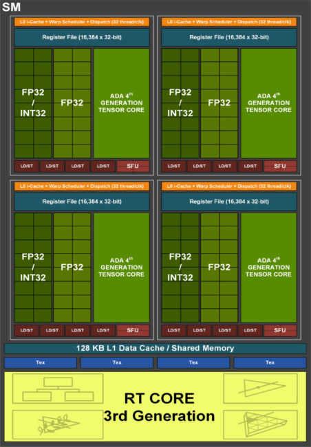
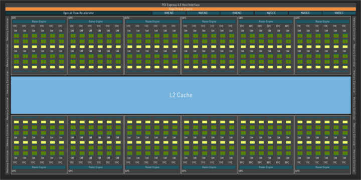
Each cache level introduces some latency, but this allows for more storage capacity. When designing the GeForce RTX 40 series graphics cards, NVIDIA found that using a single large L2 cache was faster and more efficient than other alternatives, such as smaller L2 caches combined with a Larger but slower to access L3 cache.
When operating, the GPU first looks for data in the Level 1 (L1) cache located in the SM. If the data is found in the L1 cache, there is no need to access the L2 cache. If the data is not found in the L1 cache, this is called a “cache miss” and the search continues in the L2 cache. If the data is found in the L2 cache, this is called an L2 cache hit, and the data is passed to the L1 cache and then to the processing cores.
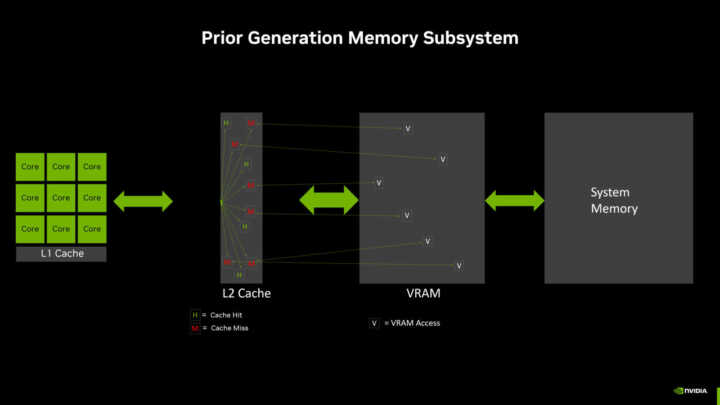
If the data is not found in the L2 cache, the GPU tries to get it from VRAM. We can observe several L2 “cache misses” in the previous diagram, which represents the memory subsystem of the previous architecture, and this leads to several accesses to the VRAM.
If the data is not present in VRAM, the GPU requests it from system memory. If the data is also not in system memory, it can usually be loaded from a storage device like an SSD or HDD. The data is then copied to VRAM, L2 cache, L1 cache and finally passed to the processing cores. It is important to note that there are different hardware and software strategies for keeping the most useful and reused data in the caches.
Each additional operation to read or write data through the memory hierarchy slows performance and consumes more power. Increasing the cache hit rate improves frame rates and efficiency.
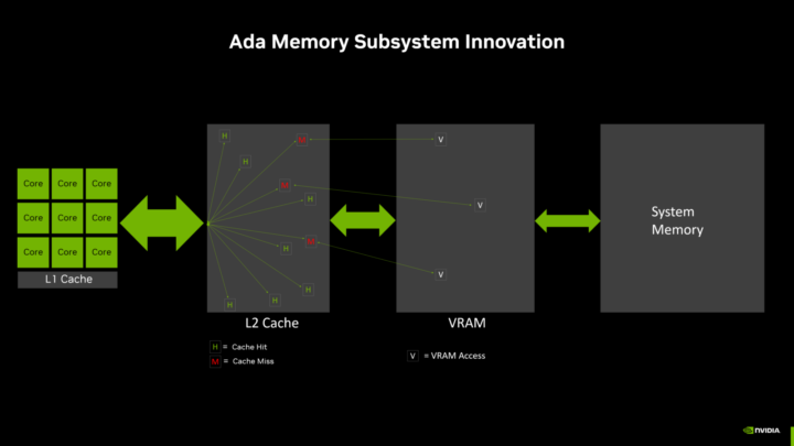
Compared to previous generation GPUs with 128-bit memory interface, the new NVIDIA Ada Lovelace architecture memory subsystem increases the L2 cache size by 16 times, which greatly improves the cache hit rate. In the previous examples, which compare Ada GPUs with previous generation GPUs, the success rate is much higher with Ada. Combined with this size, the L2 cache bandwidth of Ada GPUs has been increased compared to previous GPUs. This allows more data to be transferred between the processing cores and the L2 cache, as quickly as possible.
As shown in the diagram below, NVIDIA engineers tested the RTX 4060 Ti with its 2MB L32 cache against a special test version of the RTX 4060 Ti using only a 2MB L2 cache, which represents the L2 cache size of previous generation GPUs with a 128-bit memory interface (where 512 KB of L2 cache was associated with each 32-bit memory controller).
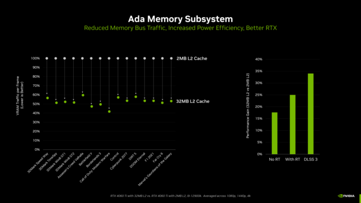
In tests with various games and synthetic benchmarks, the 2 MB L32 cache reduced memory bus traffic by more than 50% on average compared to the performance of a 2 MB L2 cache. to VRAM in the Ada memory subsystem diagram above.
This 50% reduction in traffic allows the GPU to use its memory bandwidth twice as efficiently. So in this scenario, isolating memory performance, an Ada GPU with a maximum memory bandwidth of 2 GB/s would perform similarly to an Ampere GPU with a maximum memory bandwidth of 288 GB/s. In a variety of gaming and synthetic tests, dramatically improved cache hit rates improve frame rates by up to 554%.
Memory bus width is an aspect of the memory subsystem
Traditionally, memory bus width has been used as an important metric to determine the speed and performance class of a new GPU. However, bus width by itself is not enough to indicate memory subsystem performance. It is therefore useful to understand the overall design of the memory subsystem and its overall impact on gaming performance.
Thanks to advances in Ada architecture, including new RT and Tensor cores, higher clock speeds, new OFA engine, and Ada's DLSS 3 capabilities, the GeForce RTX 4060 Ti is faster than cards previous-generation graphics, namely the GeForce RTX 3060 Ti and RTX 2060 SUPER, both of which had a 256-bit memory bus, all while consuming less power.
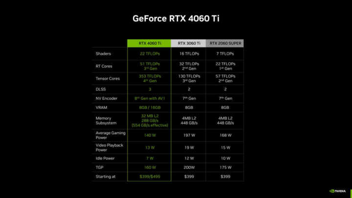
It's important to note that the performance boost doesn't just come from the increased memory bus width, but also from other GPU architecture and feature enhancements. These overall memory subsystem improvements, combined with other key features of the Ada architecture, result in higher performance and better power efficiency.
In summary, it is not necessary to limit oneself to considering only the width of the memory bus to evaluate the performance of a graphics card. It is important to consider the entire memory subsystem, as well as other features and enhancements made by the GPU architecture, in order to fully understand its impact on gaming performance.
The amount of VRAM depends on the GPU architecture
VRAM amounts on graphics cards are determined by the GPU architecture. The latest generation GDDR6X and GDDR6 memories are available with densities of 8 Gb (1 GB of data) and 16 Gb (2 GB of data) per chip. The capacity of each graphics card depends on the number of memory chips used and the width of the memory bus. For example, on the new GeForce RTX 4060 Ti GPUs with a 128-bit memory bus, the 8GB model uses four 16Gb memory chips, while the 16GB model uses eight 16Gb chips.
It is important to note that the capacity of VRAM does not only depend on the width of the memory bus, but also design choices made by the graphics card manufacturer based on targeted performance and cost of production.
Some apps may use more VRAM
Beyond gaming, GeForce RTX graphics cards can be used for 3D design, video editing, motion design, photography, architectural visualization, science, streaming, and artificial intelligence. Some of the applications used in these industries can benefit from more VRAM. For example, when editing 4K or 8K video in Premiere, or creating complex 3D scenes in 3DSMAX.
Do On-Screen Display (OSD) tools accurately report VRAM usage?
Testers often cite the "VRAM usage" metric in on-screen performance measurement tools. However, this figure is not entirely accurate, as all games and game engines work differently.
In the majority of cases, a game allocates VRAM for itself, telling your system, "I want it in case I need it." But the fact that VRAM is allocated does not mean that it is actually used in full. In reality, games will often require more memory if there is any available.
Due to how memory works, it is impossible to know precisely what is actually being used unless you are the game developer with access to the developer tools. Some games offer a preview of the amount of VRAM needed when setting graphics options, but even that isn't always accurate.
The amount of VRAM actually needed will vary in real time depending on the scene and what the player is seeing.
Additionally, games behavior may vary when VRAM is actually used to the max. In some games, memory is purged causing a noticeable drop in performance while the current scene is reloaded into memory. In other games, only certain data will be loaded and unloaded, with no visible impact. And in some cases, new items may be loaded more slowly because they are now retrieved from system memory.
For gamers, the only way to really understand how a game behaves is to play. Players can view frame rate metrics 1% low“, which can help analyze the actual gaming experience. The “1% low” metric – present in the performance overlay and logs of theNVIDIA Frame View app, as well as in other measurement tools – measures the average of the slowest 1% image builds over a period of time. If the number is too high, the viewing experience is not optimal.


